
80XXXXXX55
Send MessageStreet Address: RL-37, NEAR AIMS HOSPITAL, , MILAP NAGAR, MIDC, DOMBIVLI (EAST)
City: THANE
Province/State: Maharashtra
Country: India
Business Details: Our total strength is 80, which includes 19 engineers in cross domain expertise – electrical, electronics, mechatronics & software. We have solid electrical engineering background with 3 electrical engineers having experience of over 30 years each! We have 38 technicians who are employed in operations. Our chief of after-sales-service has 38 years of relevant industry experience. The head of operations where control panels are built is an electrical engineer from VJTI Mumbai (with scholarly records) and Masters in Science from University of Houston. We have dedicated staff of qualified and experienced engineers & technicians for after-sales-service. We have 3 modern factories (2 in Dombivali near Mumbai and 1 in Murbad) with extra-ordinary tools normally not used by competing companies. SureView has developed at least 3 products which are designed & manufactured first time in India.
Business Type: Manufacturing
Keywords: Pulsed Electric Field Generator Fuel cell Test Equipment Internet of Things Industry 4.0 Data Loggers Test Equipment as per IEC
Office Location: Maharashtra

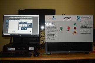
SureView has developed an automated inspection system for Semi-conductor wafers (chips) based on Machine Vision. This equipment is made to: 1. Detect & Record the Wafer ID (using optical character recognition) 2. Detect & Quantify Scratches (length, region) 3. Detect & Quantify edge chips (V grooves) 4. Detect Dies, Patches & finger-prints 5. Measure Wafer diameter and length from tapered end to centered Based on the pass/fail criteria, the equipment makes the automated inspection using computer vision and separates the good chips from defective ones. The algorithm takes less than a second to perform the inspection. Thus, the user is able to get an instant result, instead of manually performing the inspection. The system has Automatic Gain Control for different wafer surfaces and Fully automated illumination control for different defect detection: bright, dark and low angle. The lighting & setup is self-calibrated. The user readily gets the length & location of the scratch, percentage coverage area compared to the whole wafer representation on a wafer map, dimensions of the chip and information of mechanical breakage/damage of the semi-conductor wafer. The algorithm is trained to reject fingerprint stain on wafers, if any.